
I recently came across a type of device known as the writerDeck. Simply put, writerDecks are modern, computerized typewriters. I’ve been interested in typewriters for quite some time, but ink ribbons for some of these older machines can be quite expensive. That’s why the concept of a writerDeck piqued my interest when I first read about it. Since I’ve also been tinkering with microcontrollers lately, I decided to build my own writerDeck. The first step in this journey consists of building the most important part of this machine: the keyboard.
For those interested: the schematics below were made in KiCad.
A first attempt
So I decided to design and build my own mechanical keyboard. This means I need a way to connect a bunch of keyboard switches to a microcontroller. Keyboard switches are, as the name suggests, physical switches that sit underneath the keycaps. They are open by default and close when we press that key.
Our first idea might be to connect each individual switch directly to the microcontroller, like this:
We could then set each connected GPIO pin to a pin mode called INPUT_PULLUP and continually check whether any of them are reading LOW. This would indicate the connected key is being pressed (pull-up resistors are explained in more detail later on). Simple enough, right?
But there’s a problem: we’d run out of GPIO pins very quickly. To put it into perspective: the Raspberry Pi Pico has 26 multifunction GPIO pins, while a typical 60% ANSI keyboard has 61 keys.
The keyboard matrix
The solution to this problem is the so-called keyboard matrix. Instead of wiring each switch directly to a microcontroller pin, we arrange the switches in a grid of rows and columns:
Each switch can be uniquely identified by the combination of a row and a column number. Now, instead of needing one GPIO pin per key, each row and each column only requires a single pin. This means a 60% ANSI keyboard, which has 61 keys, can be handled with just 19 GPIO pins for 5 rows and 14 columns. Technically we could optimize this by having an 8×8 layout, requiring only 16 pins. But this kind of layout might not result in a pleasant typing experience.
In general, the math looks like this:
- Maximum number of keys (assuming all are 1u in size):
rows × columns - Number of GPIO pins needed:
rows + columns
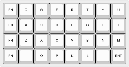
I made a provisional keyboard layout for my writerDeck, which currently looks like this:
And its corresponding matrix schematic looks like this:
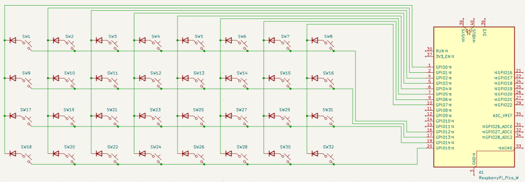
As you can see, for 32 keys, the matrix approach reduces the GPIO pin requirement to just 12 pins (4 rows and 8 columns). This is much more manageable than requiring 32 pins. The reason for the diodes next to the switches will be explained later in this post.
Reading the matrix
We can detect key presses by checking whether a closed circuit exists between particular row and column pins. The following program demonstrates how this can be done (note that debouncing is not implemented):
for (int c = 0; c < NUM_COLS; c++) {
  // Set all column pins to INPUT (high-impedance)
  pinMode(colPins[c], INPUT);
}

for (int r = 0; r < NUM_ROWS; r++) {
  // Set all row pins to INPUT_PULLUP
  pinMode(rowPins[r], INPUT_PULLUP);
}

// This loop scans the whole keyboard matrix once
for (int col = 0; col < NUM_COLS; col++) {
  // Scan one column at a time by driving it LOW (connecting to ground)
  pinMode(colPins[col], OUTPUT);
  digitalWrite(colPins[col], LOW);

  // Check each row pin for a closed circuit
  for (int row = 0; row < NUM_ROWS; row++) {
      if (digitalRead(rowPins[row]) == LOW) {
          // Key at (row, col) is being pressed (= switch is closed)
      }
  }

  // Set column back to INPUT
  pinMode(colPins[col], INPUT);
}
So at any point in time during the loop, one column is being scanned which means that column pin is connected to ground. The other column pins are like a dead end. Each row pin is pulled high by an internal pull-up resistor. So if all switches are open (i.e. no keys are being pressed), all row pins will read HIGH. The only way for a row pin to read LOW is for there to be a path from that row pin to ground (through some column pin).
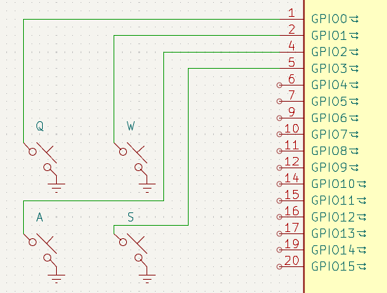
Let’s take a look at a particular scenario (the purple color represents current):
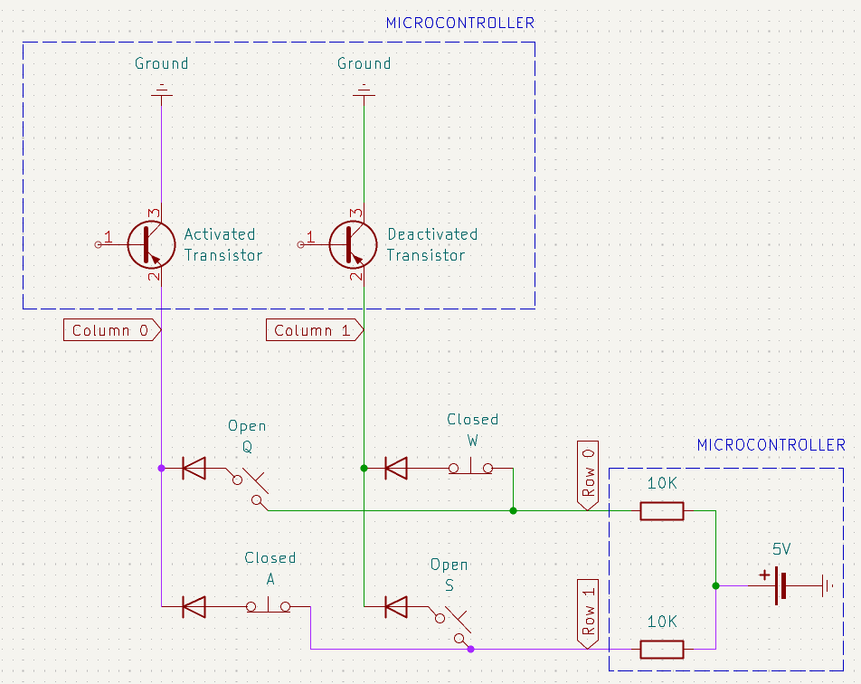
It’s important to note that when a certain column is being scanned (i.e. its pin is set to LOW), the transistor for that column is activated (which allows current to pass through). This in turn connects the column pin to ground. When a column is not being scanned (i.e. its pin is set to INPUT), the transistor is deactivated and the pin is not connected to ground (in other words: the pin is a dead end), so there exists an open circuit between every row pin and this column pin even if all keys are being pressed.
Let’s walk through what’s happening in the above snapshot:
- When a switch is open, no current flows between the corresponding row pin and column pin. This is the case with the switches Q and S in the schematic above. According to Ohm’s law, the voltage drop across the pull-up resistor (labeled as 10K in the schematic above) is zero because there is no current: $V_{drop} = I \cdot R_{pull-up} \iff V_{drop} = 0 \cdot R_{pull-up} \iff V_{drop} = 0$. This means the full supply voltage (e.g. 5V or 3.3V) remains at the row pin such that the row pin reads HIGH.
- If a switch is closed, but its corresponding column is not being scanned, current still won’t flow. This is the case with switch W. The column pin is then set to
INPUT, meaning it’s in a high-impedance (Hi-Z) state. This means the column pin is basically a dead end that isn’t connected to ground. Because there is no closed circuit, the corresponding row pin remains HIGH. - But when we scan a column by setting its pin to
OUTPUTand driving itLOW(i.e. connecting the pin to ground), any closed switch (like switch A) in that column creates a closed circuit from the corresponding row pin to ground. In that case, the row pin reads LOW, and we detect the keypress. We can illustrate this by using Ohm’s law again: $V_{supply} = I \cdot R_{pull-up} \iff I = \dfrac{V_{supply}}{R_{pull-up}} \Longrightarrow V_{drop} = \dfrac{V_{supply}}{R_{pull-up}} \cdot R_{pull-up} \iff V_{drop} = V_{supply}$ This means all of the supply voltage is dropped over the pull-up resistor such that the row pin is at 0V or LOW.
So a key press is registered when the switch is closed (i.e. we press the key) and the corresponding column is being scanned. The scanning happens so fast that we won’t “miss” any key presses (although it is theoretically possible). Whenever these two conditions are met, current will be able to flow from the corresponding row pin through the column pin to ground, which will cause that row pin to read LOW according to Ohm’s law.
We can call this active-low scanning, because whenever a row pin reads LOW, we know the key corresponding to that row and the scanned column is being pressed.
When I first learned about this, I wondered: Why not just set the columns to HIGH one at a time, set the rows to INPUT LOW, and check if any row reads HIGH (we could call this active-high scanning)? The answer is: you could, but a lot of microcontrollers don’t support a pull-down pin mode (which means they don’t provide internal pull-down resistors on the pins). If we would just set the row pins to INPUT without pull-down resistors, there would be noise and thus wrong detections would occur (because these pins would be floating). So one of the reasons active-low scanning is preferred, is because most microcontrollers have internal pull-up resistors which we can make use of.
Why use diodes?
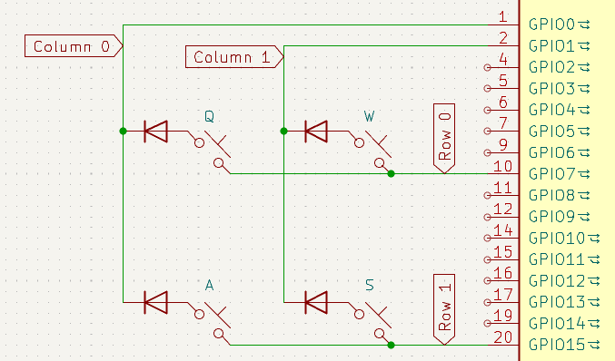
Suppose we built a keyboard matrix without any diodes, and we press three keys simultaneously:
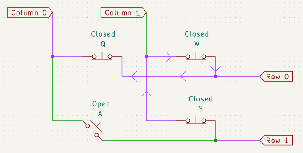
If column 0 is scanned at that moment, the microcontroller will incorrectly detect key A as being pressed, even though we didn’t press it. Why? Because there’s a path from row 1 to column 0 through the closed switches S, W, and Q. This unintended key detection is known as ghosting. To prevent this, we add a diode to each switch in the matrix:
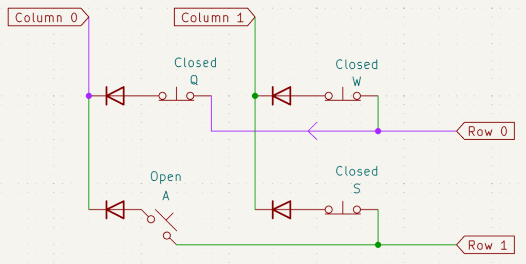
The diodes allow current to flow in only one direction, which blocks those unintended paths. The earlier path is not possible anymore as the diode at switch W would block the current coming from row 1. As a result, ghosting is eliminated.
Conclusion
There’s much more to designing a mechanical keyboard than what I’ve covered here, but these are some of the most fundamental concepts. I hope this post has helped clarify a few questions you might have while learning about keyboard matrices. The next step in building my writerDeck will be designing the case using CAD software.